|
|
|
|
|
Intel Core I7: Nehalem Arrives |
|
Join the community - in the OCAU Forums!
|
Architecture Continued
QUICK PATH INTERCONNECT AND ON-DIE MEMORY CONTROLLER
The new point-to-point interconnect and the on-die memory controller are the most significant changes over the previous system architecture. For years Intel kept instructions and data flowing to the processor through an external bi-directional data bus called a front-side bus (FSB). This bus performed as a backbone between the processor cores and a chipset that contained the memory controller hub and served as the connection point for all other buses (PCI, AGP, etc.) in the system. Previously the memory controller was located off-die and had to communicate with the processor via the front-side-bus. Although Intel has continuously increased FSB performance by pushing FSB frequency to finally 1600 MHz, the FSB architecture had became a bottleneck for system performance due its bandwidth limitation and high (meaning bad) latency.
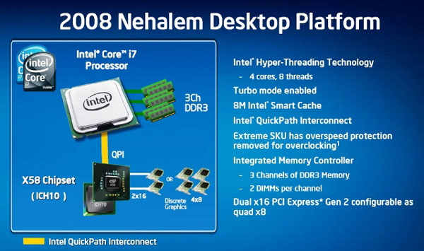
Nehalem is moving beyond FSB to a new system architecture that integrates a memory controller into each microprocessor, dedicates specific areas of system memory to each processor, and connects processors and other components with a new high-speed interconnect. Moving the memory controller on-die means that Intel is replacing the FSB architecture with a far more efficient solution. Intel had been tentatively using the name Common System Interface or CSI for the new platform architecture. This has been changed to the name Quick Path Interconnect or QPI. It provides high-speed connections between microprocessors and external memory, and between microprocessors and the I/O hub that handles traffic between processor and PCIe slots.
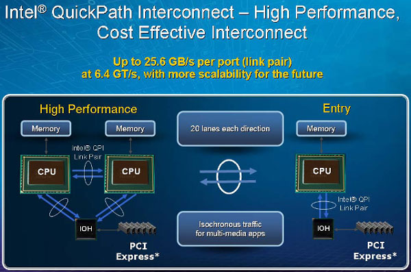
One of the biggest changes that come with QPI is the implementation of scalable shared memory. Instead of using a single shared pool of memory connected to all the processors in a server or high-end workstation through FSBs and memory controller hubs, each processor has its own dedicated memory that it accesses directly through an integrated memory controller on the processor die. In cases where a processor needs to access the dedicated memory of another processor, it can do so through a dedicated QPI that links all the processors. Unlike the previous front-side-bus, QPI is point-to-point. There is no single bus that all the processors must use and contend with each other to reach memory and I/O. This improves scalability and eliminates the competition between processors for bus bandwidth. QPI uses up to 6.4 Gigatranfers/second links, delivering up to 25 Gigabytes/second (GB/s) of total bandwidth. Intel claims that this is up to 300 percent greater than any other interconnect solution used today.
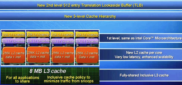
3-LEVEL CACHE HIERARCHY
Nehalem enhances the cache architecture by adding a shared L3 (last-level) cache that can be up to 8 MB in size. Nehalems L3 cache is inclusive, that means it includes all L1 and L2 data. If the core cannot find data in L3 there is therefore no need to search in L1 or L2. The redundancy is not wasting much space because the L1 and L2 caches are very small. In addition to this cache being shared across all cores, the inclusive shared L3 cache can increase performance while reducing traffic to the processor cores. Some architectures use exclusive L3 cache, which contains data not stored in other caches. Thus, if a data request misses on the L3 cache, each processor core must still be searched, or snooped, in case their individual caches might contain the requested data. This can increase latency and snoop traffic between cores. With Nehalem a miss of its inclusive shared L3 cache guarantees the data is outside the processor and thus is designed to eliminate unnecessary core snoops to reduce latency and improve performance. Nehalems three-level cache hierarchy consists of:
Same L1 cache as Intel Core microarchitecture (32 KB Instruction Cache, 32 KB Data Cache)
New L2 cache per core for very low latency (256 KB per core for handling data and instruction)
New fully inclusive, fully shared 8 MB L3 cache (all applications can use entire cache)
Notable here is that the L2 cache has become much smaller than before. It is faster though: It took 15 cycles to take data out of Penryns L2 caches. With Nehalem it is done with 10 cycles. The huge shared L3 cache becomes necessary for a monolith quadcore design but also for multithreaded applications that are being worked on by all cores.
Modern 8- and more cylinder internal combustion engines used for automobiles have the capability to shut down cylinder banks when running under low load to save fuel. Intel is using a similar technology to reduce Nehalems power consumption. Its new power control unit can disable single cores completely and reduce their power consumption close to zero when idling or in low usage.
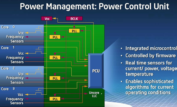
The power control unit read and processes inputs on power, current, temperature, and OS requests. It contains a PLL for each core, so that every core can be clocked individually.
IMPROVED MICROARCHITECTURE AND ADDITIONAL SSE4 INSTRUCTIONS
With the Core architecture Intel changed to a philosophy of focusing on improvements in how the processor uses available clock cycles and power, rather than just pushing up ever higher clock speeds and energy needs. The more instructions that can be run per each clock cycle, the greater the performance. Nehalem has the ability to process up to four instructions per clock cycle on a sustained basis. Intel claims that this is the best per clock cycle performance of any processor currently available.
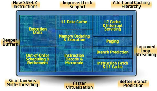
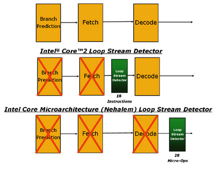
According to Intel the improved instruction per clock efficiency is the result of enhanced branch prediction, data pre-fetching, and loop stream detection as well as a variety of other changes over the existing architecture.
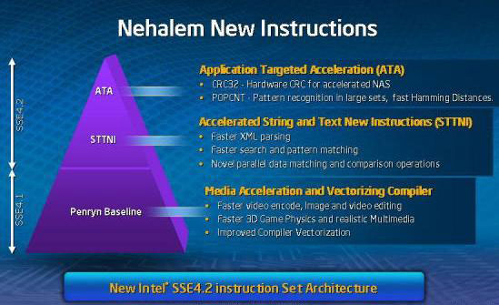
Among them are 7 additional SSE4 instructions. Nehalem includes all the additional SSE4 instructions Intel included in the previous generation Penryn for faster computation/manipulation of graphics, video encoding and processing, 3-D imaging, and gaming.
(apologies for the quality of this image)
In addition, Nehalem adds seven new Application Targeted Accelerators. They provide new string and text processing instructions to improve performance of string and text processing operations. For example, they enable parsing of XML strings and text at a much higher speed. According to Intel, the additional SSE4 instructions will be useful for lexing, tokenizing, regular expression evaluation, virus scanning, and intrusion.
|
|
Advertisement:
All original content copyright James Rolfe.
All rights reserved. No reproduction allowed without written permission.
Interested in advertising on OCAU? Contact us for info.
|

|