|
|
|
|
|
AMD Trinity A10-5800K & GIGABYTE F2A85X-UP4 |
|
Join the community - in the OCAU Forums!
|
Introduction, Platform Overview
AMD's Trinity APU (Accelerated Processing Unit) is not news - it was launched for laptops, as part of the 'Sabine' platform, in May last year. But more recently it has been released for desktop use, which makes it more interesting to enthusiasts. APU is a term coined by AMD to differentiate their long heralded 'Fusion' chips from the discrete equivalents they are built from - such as the FX line of CPU's, and Radeon line of GPU's.
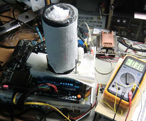
Most users on OCAU enjoy gaming, so this review is concentrated on just that. Read on for: a brief recap of the new APU's, including the A10-5800K that will be tested, an introduction to a new chipset, an accompanying new motherboard from Gigabyte, some overclocking (including a little bit of dry ice, sub-zero OC), and then some gaming results.
Platform Overview
The desktop APU form factor allows AMD to bump up the TDP (Thermal Design Power) from the battery-constrained 17-35W laptop range to a more lively 65-100W spread. The extra power headroom has been used to twist the clock speed knob around a few notches.
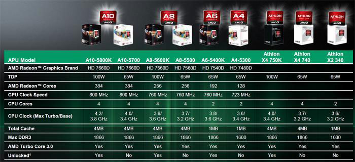
While the laptop chips topped out at 3.2GHz turbo speeds for the CPU, the slowest desktop chip (the A8-5500) has that as the base frequency, and turbo speeds climb up to a peak of 4.2GHz in the flagship A10-5800K model, which will be tested in this review. Similarly the GPU frequencies have gone up from a maximum of 496MHz, to 800MHz.
Another important difference is official support for DDR3-1866, and as other reviews around the net have shown (as well as forum posts from booj and mAJORD), memory speeds are crucial to eking extra performance from the GPU.
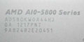
AMD A10-5800K
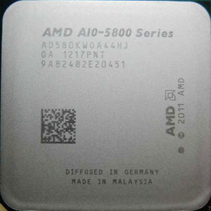
Top of the Trinity tree is the A10-5800K. AMD have borrowed the 'K' suffix from Intel in recent times, and in an industry of regularly bizarre model names, it amazingly means the same thing an unlocked clock speed multiplier. For the uninitiated, this feature allows the end user to further twist that clock speed knob in the easiest way possible, as shown later in this article.
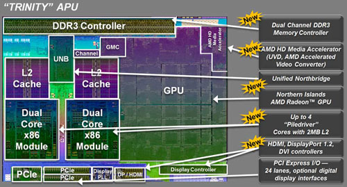
The die shot reveals that the largest block of the 246mm2 silicon real estate belongs to the GPU.
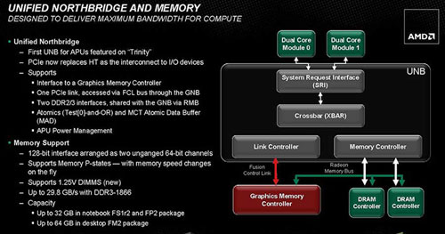
The unified north bridge is an interesting area that highlights this exciting time in chip development, in which the integration of the separate CPU and GPU elements is slowly evolving. Trinity takes this integration past the stage of being stuck next to each other, like early dual-core CPU's, but it will likely be a few more generations before we see the exciting, hardware level synthesising of the respective processing paradigms.
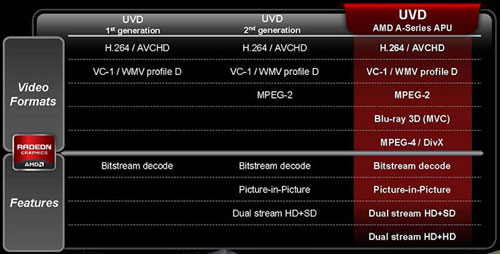
Another nifty feature is the latest version of AMD's Unified Video Decoder, UVD3, straight from the Radeon 6000 series that the graphics core of this APU is based on.
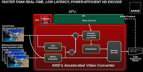
Video Codec Engine is a feature from the more recent Radeon 7000-series GPU that enables encoding H264/AVC content at 1080p at a rate of 60fps.
|
|
Advertisement:
All original content copyright James Rolfe.
All rights reserved. No reproduction allowed without written permission.
Interested in advertising on OCAU? Contact us for info.
|
|