Introduction, CPU, Chipset
'Haswell' is Intel's latest architecture. It is built on the 22nm "tri-gate" process that was introduced with last year's 'Ivy Bridge' line of processors. Even in their second processor iteration at this process geometry, over a year after the initial release, Intel still enjoys a comfortable advantage in this metric. All their competitors are stuck at the 28nm half-node, with no relief in sight until next year.
Despite this clear advantage, Intel and x86 competitor AMD have largely missed out on the big growth business of phones, tablets, 'phablets', and other portable devices. ARM processors are cheaper, and their historical emphasis on frugal power consumption, rather than the outright performance of the x86 world, is better suited to a small form factor. The success of ARM has not gone unnoticed; Intel have mounted a pretty aggressive campaign to minimise power consumption, whilst keeping their performance advantage.
Another aspect of the various ARM SoC's (System on Chip) success is the integrated graphics processing unit, or GPU. This has been the weak spot in the Intel juggernaut's armour for some time, despite steady progress in their last few processor generations. 'Haswell' continues the upward trend, bringing more shader units, higher clock speeds, and even an on-chip, high-speed 128MB eDRAM for those with (very) deep pockets.
Today OCAU brings you a review of the Intel i5 4670K CPU, along with a look at the Z87 MPOWER motherboard from MSI. Instead of the typical plethora of synthetic CPU benchmarks, this article will focus on the gaming capabilities of Haswell. Have Intel's graphics caught up to the competition from AMD? Does the chip continue the stellar overclocking potential of Ivy Bridge? How does the MSI motherboard fare with some OC punishment? Read on for details.
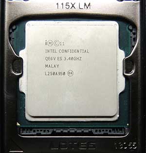
Intel Core i5 4670K:
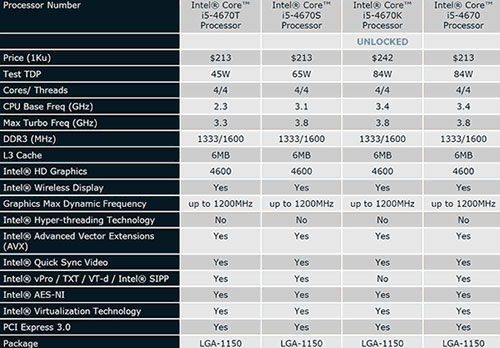
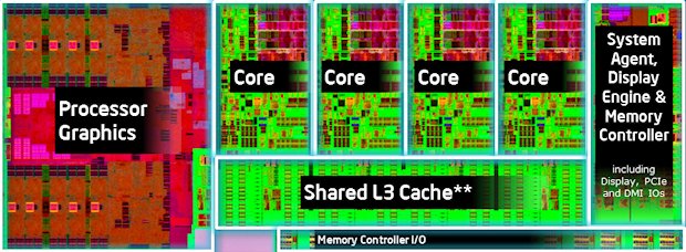
The 4670K has OC 'cheat mode' enabled straight out of the box: the unlocked multiplier. It runs at a nominal clock speed of 3.4GHz, which turbo can ramp up to 3.8GHz. Being a cheaper i5 mean it misses out on HyperThreading, which is only present in Core i7 products. L1 data cache is 128kB (32kB per core), as is L1 instruction cache. L2 cache is 1MB (256kB per core). As the diagram above explains, load and store bandwidth in the L1 data cache have both doubled since Sandy Bridge, as has the L2 bandwidth to L1.
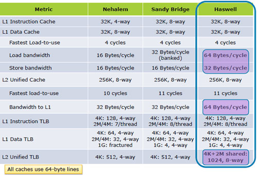
The L2 Unified Transition Lookaside Buffer (TLB) now has a 2MB shared page which should assist cores in finding data or instructions from the cache of other cores, without going out to RAM. L3 cache is 6MB. The SKU's with stacked eDRAM use it as an L4 cache.
Unfortunately, what the Intel giveth, the Intel taketh away; the 'K' chips have all virtualisation features disabled, and they also miss out on possibly the most interesting feature of the Haswell microarchitecture, transactional memory or TSX. For deeper analysis, check out David Kanter's article here. He also writes a thorough analysis of the Haswell architecture here.
It seems questionable that the most expensive Core i5 and Core i7 chips don't come with the full list of features, but that's marketing, and for a Haswell chip with an unlocked multiplier it's an unavoidable reality.
Z87 Chipset:
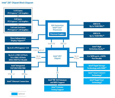
The Z87 chipset is the top dog of LGA 1150 chipsets, targeted at enthusiasts. It's pretty feature packed but not a great deal different from the preceding Z77.
|