|
|
Advertisement:
|
|
NVIDIA's GeForce GTX 580 vs GTX 480 |
|
Join the community - in the OCAU Forums!
|
Introduction, Features
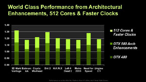
The 500-series of video cards came as a surprise from NVIDIA in both naming and performance. With the GTX 480 being originally delayed and not being as refined as people had hoped, NVIDIA has come back later this year with a new naming scheme and a promise to fix its wrongs with the GTX 480. Today we take a look at NVIDIA's new flagship GTX 580 graphics processor and see how it compares to the previous GTX 480 in the usual gauntlet of benchmarks, plus some new inclusions like Just Cause 2 by developer Eidos and BitSquid's Stone Giant benchmark.
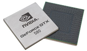
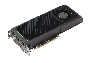
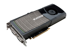
NVIDIA's GeForce GTX 580 measures in at 267 millimetres in length (10.5 inches) like the GTX 480, and requires a minimum of 600W or greater system power supply. Cooling is provided by a redesigned NVIDIA solution with a centrifugal-type fan and vapor heat sink. As with all high-end NVIDIA graphics cards it features support for NVIDIA's SLI multi-GPU technology, 3D Vision, 3D Vision Surround (two cards required), CUDA technology, PhysX acceleration and Microsoft DirectX 11 game support, as well as a variety of video enhancement technologies under the NVIDIA PureVideo HD umbrella.
Fundamentally the GTX 580 shares the same architecture as the GTX 480, but NVIDIA's engineers have improved on the texture filtering speeds and improved Z-culling. Z-culling is a method of improving performance by getting rid of pixels that won't be seen as they are behind an object or building, thus reducing the amount of rendering required in a scene. They also increased/unlocked a further 32 CUDA cores (disabled in the GTX 480) increasing the total to 512. Meanwhile, engineers refined and tweaked the GPU at silicon level to reduce the amount of leaky transistors allowing it to move away from the GTX 480's power troubles, and help in overall power savings which are now seen in the GTX 580, as well as higher default clocks at a low thermal design power (TDP).
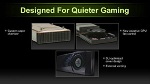
While the hardware was being refined and optimised, NVIDIA's engineers starting working on the cooling solution. With reports about the GTX 480 being overly hot and loud when released earlier this year, NVIDIA knew that things couldn't be left in that manner. So they went back to the drawing board and beefed up the cooling with a vapor chamber heat sink design, optimised the fan speeds, tweaked the fan design, and reduced the amount of heat the video card dissipated inside the case.
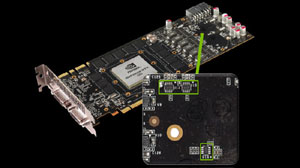
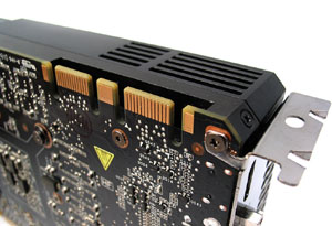
A new feature found in the GTX 580 is a set of hardware monitoring chips (highlighted below). These chips offering real-time monitoring of current and voltages on each 12V rail (8-pin, 6-pin and PCI-Express) and make sure the video card doesn't exceed its maximum power usage rating. While this implementation does not cause any issues for gaming and benchmarking scenarios that we are aware of, its purpose is to stop programs like Furmark and OCCT over stressing the card outside of general usage scenarios. Why these programs? Apparently both NVIDIA and AMD see them as power 'viruses' that don't represent real-world values.
Now to the design; to the left you can see the new design of the GTX 580, and to the right is the older GTX 480. The new GTX 580 refrains from the use of a exposed heat sink design to dissipate extra heat produced by the GPU, and no heat pipes are present on the top of the card anymore leading to a more refined look, and one that is less prone to radiating heat to adjacent cards.
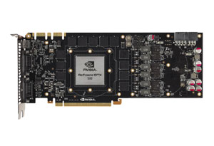
Not much has changed in terms of PCB layout below, apart from the alignment of the memory chips and the removal of a couple of capacitors. The most obvious difference is the exclusion of cut-outs in the PCB to allow more air to be sucked in by the original GTX 480 fan. Due to the new cooler design and lower power requirements these holes in the PCB are no longer required.
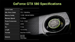
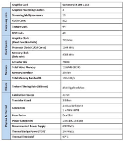
Below is a more detailed list GTX 580 specification list as provided by NVIDIA. The biggest change in the hardware comes with the unlocking of the 16th streaming processor unit, pushing the amount of CUDA cores to 512 (vs. 480) and texture units to 64 (vs. 60) compared to the GTX 480.
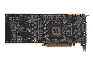
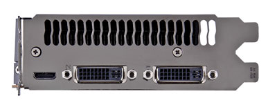
NVIDIA's GeForce GTX 580 conforms to the same set of connectors we found on the GTX 480. These include a pair of dual-link DVI outputs along with a mini-HDMI (version 1.4a) output header. Unfortunately bitstreaming support for Dolby True HD and DTS-HD Master Audio over HDMI is not present as with the GTX 480.
On the top of the card we find a dual SLI connectors; unlike mainstream video cards such as the GTX 460 and 450, the GTX 580 supports 3-way SLI, and up to 4-way SLI with supporting boards, just as on the GTX 480 previously.
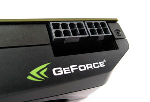
At the end of the card there are a pair of PCI-Express power connectors, one is a 6-pin and the other an 8-pin. This is unchanged from the GTX 480, even though the card draws less power during normal gaming situations.
With the introduction of the GTX 580, NVIDIA have released two new demos to show off the DirectX 11 tessellation performance of its new flagship video card. The first demo is called Endless City and shows off an impressive amount of geometric details in an NVIDIA-designed city. The second is called Alien vs. Triangles and expands the use of tessellation to moving objects and not just stationary environments. While the demos suggest a GTX 500-series is required, we had no problem in using them with 400-series products. So give them a whirl!
|
|
Advertisement:
All original content copyright James Rolfe.
All rights reserved. No reproduction allowed without written permission.
Interested in advertising on OCAU? Contact us for info.
|
|